Thermal Detector Packaging & Assembly
At Landmark Engineering, we are proud to introduce our newest capability: advanced thermal detector packaging. This expansion builds upon our established expertise in optics manufacturing, allowing us to provide end-to-end solutions for thermal imaging systems. By integrating state-of-the-art cleanroom facilities and precision machinery, we now offer comprehensive packaging services for thermal imager detector chips. These services support our internal projects while extending to external clients who require high-reliability, custom packaging solutions tailored to their specific needs.
Our Expertise in Thermal Detector Packaging
Thermal detector packaging is a critical step in ensuring the longevity, performance, and environmental resilience of infrared sensors. Our dedicated cleanrooms are equipped with vacuum chambers, temperature-controlled environments, and automated systems designed to meet the stringent demands of hermetic sealing and component integration. We specialize in packaging focal plane array (FPA) dies, which form the core of thermal imagers used in applications such as commercial imaging, thermography, scientific research, and medical diagnostics.
Our processes adhere to industry-leading standards, including ISO certifications for quality management and cleanroom operations (Class 100/ISO 5). This ensures contamination-free assembly, minimizing defects and maximizing yield rates for both prototype development and mid-volume production.
Key Capabilities and Processes
We employ a suite of advanced techniques to deliver robust, vacuum-sealed detector packages. Our capabilities include:
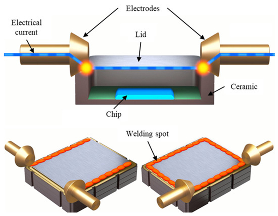
– Vacuum Welding and Laser Welding: Precision joining of components under controlled vacuum conditions to create hermetic seals that protect against moisture, gases, and environmental stressors.
– Getter Activation: Integration and activation of getters to maintain ultra-low vacuum levels inside the package, enhancing long-term stability and sensor performance.
– Glass-to-Metal and Metal-to-Ceramic Welding: Specialized bonding methods that ensure seamless interfaces between diverse materials, reducing thermal mismatch and improving mechanical integrity.
– Wire/Die Bonding: High-precision gold wire bonding for reliable electrical connections between the FPA die and package leads, supporting high-speed data transmission.
– Wafer Dicing/Grinding/Polishing: Accurate singulation of wafers into individual dies, with options for custom sizes and edge treatments to prevent chipping or contamination.
– Additional Services: Custom hermetic encapsulation, thermal cycling testing, and leak detection to verify package integrity.
These processes are scalable, accommodating everything from small-batch prototypes to medium-scale production runs, with turnaround times optimized for efficiency without compromising quality.
Technical Example: LWIR Detector Packaging
For long-wave infrared (LWIR) applications, our packaging process leverages premium materials and components to achieve superior thermal and optical performance.
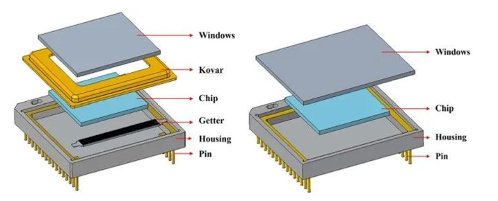
1. FPA Die: The sensitive focal plane array sensor, carefully mounted to minimize stress and ensure flatness.
2. Ceramic/Kovar Base Package: Provides a stable, thermally matched foundation with excellent hermetic properties.
3. Kovar Cap: A durable lid for enclosure, welded to the base for airtight sealing.
4. Ge/Si Window: Optically transparent materials selected for their infrared transmission efficiency and durability in harsh conditions.
5. Getter: Absorbs residual gases to sustain vacuum integrity over the device’s lifecycle.
6. Gold Wire for Wire Bonding: Ensures low-resistance, reliable interconnections.
7. Indium Solder Sheets: Used for low-temperature soldering, ideal for temperature-sensitive components.
This configuration results in detectors that operate effectively across wide temperature ranges (-40°C to +85°C) and exhibit low noise equivalent temperature difference (NETD) for high-resolution imaging. Our in-house testing protocols, including helium leak detection and thermal shock cycling, guarantee compliance with MIL-STD specifications.
Why Choose Landmark Engineering for Detector Packaging?
– Innovation and Integration: As a full-service provider, we seamlessly combine our optics manufacturing fame with detector packaging, enabling complete thermal imaging assemblies from a single source. This reduces supply chain complexities and accelerates time-to-market for your products.
– Cost-Effective Solutions: Our efficient processes and economies of scale deliver high-quality packaging at competitive prices, whether for in-house use or as a contract service.
– Reliability and Quality Assurance: Every package undergoes rigorous quality control, including 100% inspection and traceability from raw materials to final delivery. We prioritize customer specifications, offering customization options to meet unique application requirements.
– Client-Centric Approach: We collaborate closely with clients to understand their needs, providing engineering support from design consultation to post-production validation. Our track record in serving industries like aerospace, defense, and healthcare demonstrates our commitment to excellence.
This new sector represents a strategic milestone in Landmark Engineering’s growth, reinforcing our position as a leader in precision optics and thermal imaging technologies. By investing in cutting-edge infrastructure, we empower our clients to innovate with confidence.

Contact Us
Ready to discuss your thermal detector packaging needs? Reach out to our team today for a consultation, quote, or to learn more about how we can support your projects. Let’s build the future of thermal imaging together.